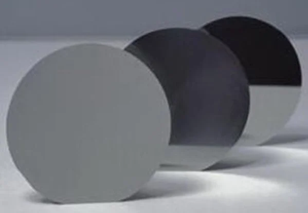
Semiconductor Wafers
Semiconductor wafers are foundational components in the electronics industry, serving as the substrate for the fabrication of integrated circuits (ICs) and other semiconductor devices. These wafers are typically thin, disc-shaped slices made from a single crystal or polycrystalline material, with silicon being the most widely used due to its excellent semiconductor properties. Silicon wafers play a pivotal role in the production of microelectronics, enabling the creation of the intricate circuitry that powers a vast array of electronic devices.
The manufacturing process of semiconductor wafers involves several critical steps. First, a single crystal ingot of high-purity sapphire, germanium, silicon or silicon carbide is sliced into thin wafers using a precision saw. These wafers undergo a series of chemical and mechanical processes to achieve a smooth, flat surface and consistent thickness. The resulting wafers serve as the canvas for the creation of semiconductor devices through photolithography, etching, and deposition processes.
Semiconductor wafers come in various sizes, with diameters ranging from a few inches to over a foot, and their dimensions play a crucial role in determining the number of devices that can be produced in a single manufacturing run. The wafer's surface is typically polished to an ultra-smooth finish to ensure uniformity in subsequent processes.
These wafers are the platform upon which intricate patterns of transistors, resistors, and interconnects are created during the semiconductor fabrication process. The properties of the semiconductor material, as well as the precision in wafer manufacturing, directly impact the performance and reliability of the electronic components produced. Semiconductor wafers are essential in driving technological advancements across various industries, from consumer electronics to healthcare, automotive, and beyond, making them a critical element in the modern digital age.
Lithium Niobate (LiNbO3) Wafers
Lithium Niobate (LiNbO3) Wafers
Lithium Niobate (LiNbO3) wafers are integral to the fields of photonics, telecommunications, and nonlinear optics due to their exceptional electro-optic, piezoelectric, and photorefractive properties. These wafers are commonly used in devices such as modulators, frequency converters, and optical waveguides. The unique properties of Lithium Niobate make it a versatile material for various applications, including surface acoustic wave (SAW) devices, optical parametric oscillators (OPOs), and Q-switches in lasers.
Available in various orientations and dopings, Firebird Optics’ Lithium Niobate wafers can be tailored to meet specific technological requirements. The wafers' ability to manipulate light and sound waves makes them invaluable for research and development in advanced optical communication systems and high-precision optical instruments. Their versatility and performance have made them a preferred choice for scientists and engineers working on cutting-edge optical technologies.
Custom sizes are available upon request. Please send your specs to info@firebirdoptics.com
Specs for Lithium Niobate (LiNbO3) Semiconductor Wafers:
Double Side Polished (DSP)
Cleaning/Packaging: Class 100 cleanroom and vacuum packaging.
Lithium Niobate Semiconductor Wafers: Versatility in Optoelectronics
Lithium niobate semiconductor wafers are critical components in the field of optoelectronics, known for their unique electro-optic, acousto-optic, and nonlinear optical properties. These wafers, made from lithium niobate (LiNbO3), are utilized in a variety of applications ranging from telecommunications to advanced photonic devices. Their ability to manipulate light and sound waves with high precision makes them indispensable in modern technology.
Properties of Lithium Niobate
Lithium niobate wafers exhibit several key properties that make them ideal for optoelectronic applications:
High Electro-Optic Coefficient: Lithium niobate can change its refractive index in response to an electric field, making it valuable in modulating light.
Nonlinear Optical Properties: These wafers can generate new frequencies of light through processes like second-harmonic generation.
Piezoelectric and Pyroelectric Properties: Lithium niobate can convert mechanical stress into electrical signals and vice versa, and it can also generate an electric charge in response to temperature changes.
Applications:
1. Telecommunications:
Lithium niobate wafers are widely used in optical modulators for fiber optic communications. Their high electro-optic coefficient allows for efficient modulation of light signals, which is essential for transmitting data over long distances with minimal loss.
2. Integrated Optics:
These wafers serve as the foundation for integrated optical circuits. Devices such as waveguides, switches, and frequency converters are built on lithium niobate substrates due to their excellent optical properties and compatibility with various fabrication techniques.
3. Nonlinear Optics:
The nonlinear optical properties of lithium niobate make it suitable for applications like second-harmonic generation, where it is used to convert laser light to different wavelengths. This is critical in laser technology and advanced photonics research.
4. Sensors and Actuators:
Thanks to their piezoelectric properties, lithium niobate wafers are used in sensors and actuators. These applications range from medical ultrasound devices to precision measurement tools in various industries.
5. Acousto-Optic Devices:
Lithium niobate is also employed in acousto-optic devices, where it is used to control light with sound waves. These devices are utilized in applications such as laser scanning, optical filtering, and signal processing.


